-
-
-
#18/9, A.R Plaza, 3rd Floor, BTM Layout, Bangaluru-560029
Welcome to Our Fixpro Office
Please fill out the form below and we will get back to you as soon as possible.
Contrary to popular belief, Lorem Ipsum is not simply random text. It has roots in a piece of classical Latin literature from 45 BC, making it over 2000 years old.
At Ana Semiconductor, we deliver highly optimized Custom Layout Design solutions for Analog, Digital, Mixed-Signal and RF circuits. Our layout team focuses on performance, reliability, low-power, DRC/LVS clean designs, and foundry-ready layouts across multiple technology nodes.
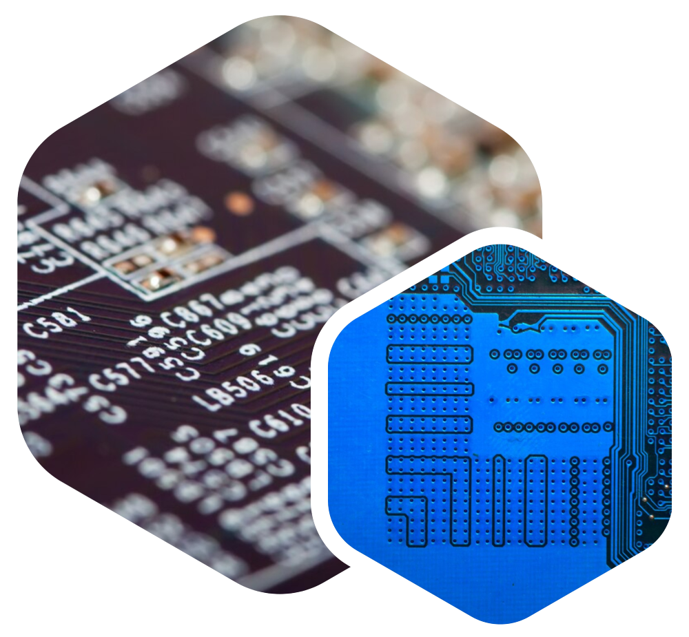
Our Custom Layout team provides end-to-end layout development from device-level placement to full chip integration. We ensure foundry-compliant, performance-driven layouts designed with minimum parasitics, excellent matching, and robust reliability.

70+ layout professionals with deep expertise in Analog, Digital, RF, and High-Voltage layout design across multiple foundries.
• Analog & Mixed-Signal Layout
• Standard Cell & Memory Layout
• RF, High-Speed & IO Layout
• Power-Aware & Low-Noise Layout Practices
• DRC/LVS/ANT/ERC Sign-off
• Parasitic Extraction (PEX)
• EM/IR & Reliability Checks
• Multi-Corner Validation
Successfully delivered layouts for:

Work with our expert layout engineers to deliver foundry-ready, high-performance IC layouts.
Get StartedWe support 7nm, 14nm, 28nm, 40nm, 65nm, 90nm, 130nm, 180nm, and high-voltage specialty nodes depending on project needs.
Yes, including block-level layout, top-level integration, routing, floorplanning, and physical verification.
Yes—common-centroid, symmetry, shielding, ESD compliance, and high-speed routing best practices are strictly followed.
• Cadence Virtuoso
• Synopsys Custom Compiler
• Mentor Calibre DRC/LVS
• Cadence Assura & PVS
• Parasitic Extraction Tools
Yes, including TSMC, Samsung, GlobalFoundries, UMC, TowerJazz, X-Fab and others.
Proven experience across tape-outs, high-quality layouts, strict sign-off compliance, and optimized design for performance, area, and reliability.